Comic
Fay's Diary Comic
Kanji Transformer Series
Our Android Apps
Paper Toy
Animation
Dharma Cartoon
Figure Photo Collection
Flash Game
Embedded Systems
Old Work
Toy & Gadget
Game & Software
About Us
Links
Ataya's Embedded Systems Blog
Green Tea Story
Play with BeagleBoneBlack
Studio Wallpaper
Studio Wallpaper
The Sky Flower & The Temple Dog
Date : Wednesday,11 May 2016
Writer : Ataya P
I just learned how to add Logo or Bitmap file into Kicad's PCB tool. I will show you how to do it. Let's see...
Working Platform :
Lenovo Notebook , Intel Pentium Dual Core T2080 1.73GHz
2Gbyte RAM
Ubuntu Ubuntu 12.04.3 LTS + Kicad installed
Details
1.Make your logo that is black & white base.(white color background)
2. Open Kicad and click on Bitmap2Component tool icon. Load a bitmap file.

3. On Options, Select Negative option and then click on Export to Pcbnew button.

4. Save your logo component to your project directory.

5. Open your Kicad's PCB tool, choose Preferences->Library and add your logo component into the project.

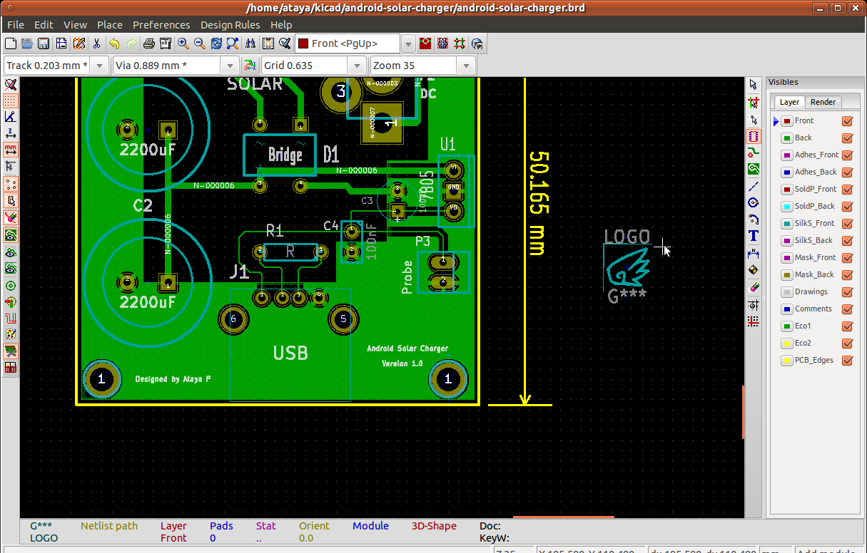
6. On PCB tool bar, select Add Modules icon and looking for LOGO
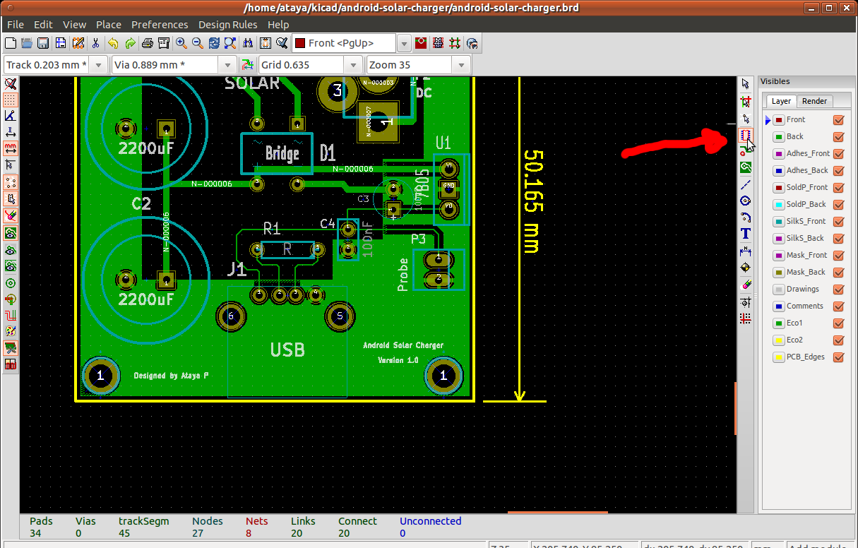

7. Then the logo will appear on your PCB but it still has bug that lines are shown on upper and left corners of the logo.
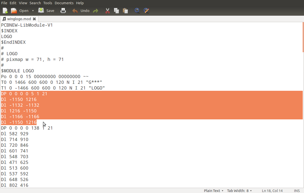
8. To fix the bug, open the logo file with text editor and delete the first DP lines as you see in image below. Save the file and reload the Kicad's PCB again.
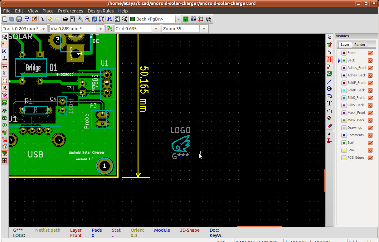
9. That is ! the bug lines are gone. Now you can add your logo on PCB.
Useful Link :
Kicad EDA website->
http://kicad-pcb.org/
Writer : Ataya P
I just learned how to add Logo or Bitmap file into Kicad's PCB tool. I will show you how to do it. Let's see...
Working Platform :
Lenovo Notebook , Intel Pentium Dual Core T2080 1.73GHz
2Gbyte RAM
Ubuntu Ubuntu 12.04.3 LTS + Kicad installed
Details
1.Make your logo that is black & white base.(white color background)
2. Open Kicad and click on Bitmap2Component tool icon. Load a bitmap file.
3. On Options, Select Negative option and then click on Export to Pcbnew button.
4. Save your logo component to your project directory.
5. Open your Kicad's PCB tool, choose Preferences->Library and add your logo component into the project.
6. On PCB tool bar, select Add Modules icon and looking for LOGO
7. Then the logo will appear on your PCB but it still has bug that lines are shown on upper and left corners of the logo.
8. To fix the bug, open the logo file with text editor and delete the first DP lines as you see in image below. Save the file and reload the Kicad's PCB again.
9. That is ! the bug lines are gone. Now you can add your logo on PCB.
Useful Link :
Kicad EDA website->
http://kicad-pcb.org/
- ataya_p's blog
- Login to post comments

Custom Search
